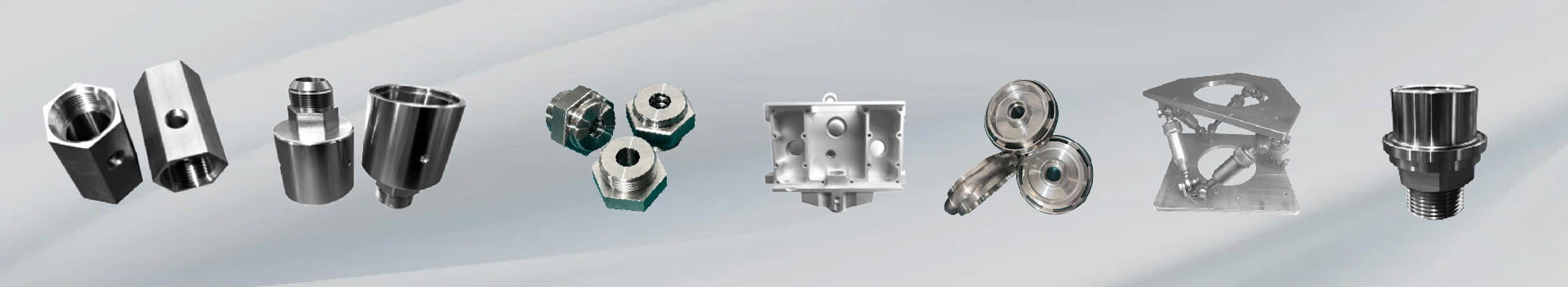
A factory specializing in custom machining of metal and plastic products in China! We provide sheet metal processing fabrication service, etc.
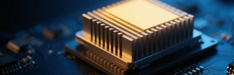
Sheet metal fabrication, CNC machining, injection molding, and stamping have diverse applications in the semiconductor industry:
Sheet Metal Fabrication Applications:
In semiconductor manufacturing, sheet metal fabrication is widely used to produce precision enclosures and structural components for equipment, such as vacuum chambers for etching systems, shielding covers for lithography machines, and wafer transfer module housings. This process ensures the creation of ultra-clean, corrosion-resistant, and vacuum-compatible parts that meet the stringent requirements of semiconductor cleanroom environments.
CNC Machining Applications:
CNC machining is critical for manufacturing high-precision components in semiconductor production equipment, including electrostatic chucks, gas distribution plates for plasma reactors, and alignment fixtures for wafer handling systems. With micron-level tolerances and complex geometries, CNC technology guarantees the accuracy and repeatability required for nanoscale semiconductor processes, directly impacting chip yield and quality.
Injection Molding Applications:
Injection molding plays a vital role in producing specialized plastic components for semiconductor devices and packaging, such as IC test socket housings, connector insulators for automated testing equipment (ATE), and protective casings for sensor modules. The process enables mass production of dimensionally stable parts with excellent dielectric properties, supporting the miniaturization and high-frequency performance demands of modern electronics.
Stamping Applications:
Metal stamping is extensively employed in semiconductor packaging and assembly, manufacturing lead frames for chip encapsulation, heat sink fins for thermal management, and precision metal masks for solder ball placement. The high-speed stamping process ensures cost-effective production of micron-scale features while maintaining consistency across millions of components, crucial for large-scale semiconductor packaging operations.
Overall, these advanced manufacturing processes form the backbone of semiconductor technology development, enabling the creation of ultra-precise, reliable, and scalable solutions for wafer processing equipment, chip packaging systems, and electronic device manufacturing. Their integration drives continuous innovation in semiconductor performance and production efficiency.
Copyright © 2026 Shanghai Jinxi Precision Machinery Co., Ltd. All rights reserved.